What is the Electrical Return Path in a PCB?
Par un écrivain mystérieux
Last updated 07 juillet 2024
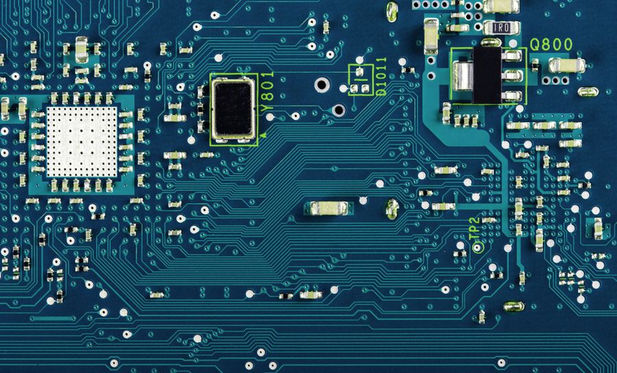
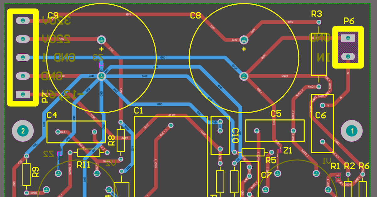
One of the fundamental aspects of any circuit diagram is the return current path or electrical return path. In a circuit diagram and a schematic diagram, the path the current follows to return to the low potential side of a power source should be obvious, but it may not be so obvious in a PCB.

An intuitive, practical approach to mixed-signal grounding - EDN
Our top 5 rules for PCB noise reduction
PCB design and ground layout considerations - VSDSP Forum

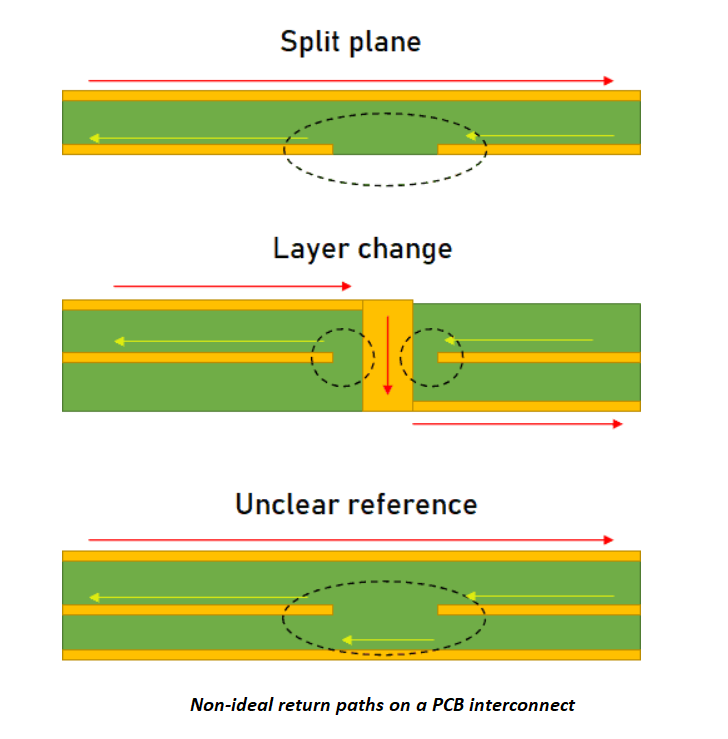
Alternative Paths of the Return Current - In Compliance Magazine
Follow Your Multilayer Ground Return Path to Prevent EMI, Blog

Design PCBs for EMI, part 3: Partitioning and routing - EDN Asia
Return Current Transition Between Planes, 2020-02-04
In-Design Return Path Analysis - Sigrity - System Analysis - Cadence Community

How to Optimize the Return Path for High-Speed PCB Signals
Recommandé pour vous
 Trace PCB: A Comprehensive Guide14 Jul 2023
 What is PCB Design14 Jul 2023
 PCB At the heart of every electronics device14 Jul 2023
 10Pcs Universal PCB Prototyping Board, Double Sides Solderable Breadboard PCB Board Tin Plated Perf Board, Electronics DIY Soldering Universal Circuit14 Jul 2023
 PCB design - from idea to dedicated prototype14 Jul 2023
 PCB Basics - SparkFun Learn14 Jul 2023
 Printed Circuit Boards: A Guide What is a PCB, Applications, Types14 Jul 2023
 All About PCB Tooling Holes: What They Are and Where They Go14 Jul 2023
 Electronic systems design and manufacturing14 Jul 2023
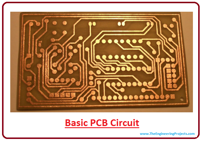 Introduction to PCB(Printed Circuit Board) - The Engineering Projects14 Jul 2023
Tu pourrais aussi aimer
 Hay Spear- By American Attachments Skid Steer14 Jul 2023
 Achat Montre connectée Garmin Venu 2S Rose Gold avec bracelet silicone blanc 010-02429-1314 Jul 2023
 Poussette Trio YOYO² pack 0+ & 6+ + siège auto YOYO car seat by14 Jul 2023
 Housse de vélo pour 2 vélos Tissu Oxford 210D imperméable de vélo14 Jul 2023
 Classeur de cartes photo Kawaii Kpop de 7,6 cm - Mini idole - Album photo esthétique - 40 pochettes (rose)14 Jul 2023
 Prci Calibreur - Ebavureur pour tube PER & multicouche 16-18 - 20-25mm, Gris : : Industrie et science14 Jul 2023
 Refroidisseur d'eau KRM rouge taillé masse14 Jul 2023
 SKITTLES14 Jul 2023
 HTOOQ 4 Pcs Bouteille de Champagne et Gobelet à Vin Ballons en14 Jul 2023
 Une Maquette Miniature Dorée Du Temple Et Un Arbre Avec Des14 Jul 2023